Visual Intelligence Summit: Oct 22 in San Francisco Get your ticket

Wafer Defect Detection AI

Classify every defect on every wafer, from the edge bevel to the die pattern, and map it to the process that made it.
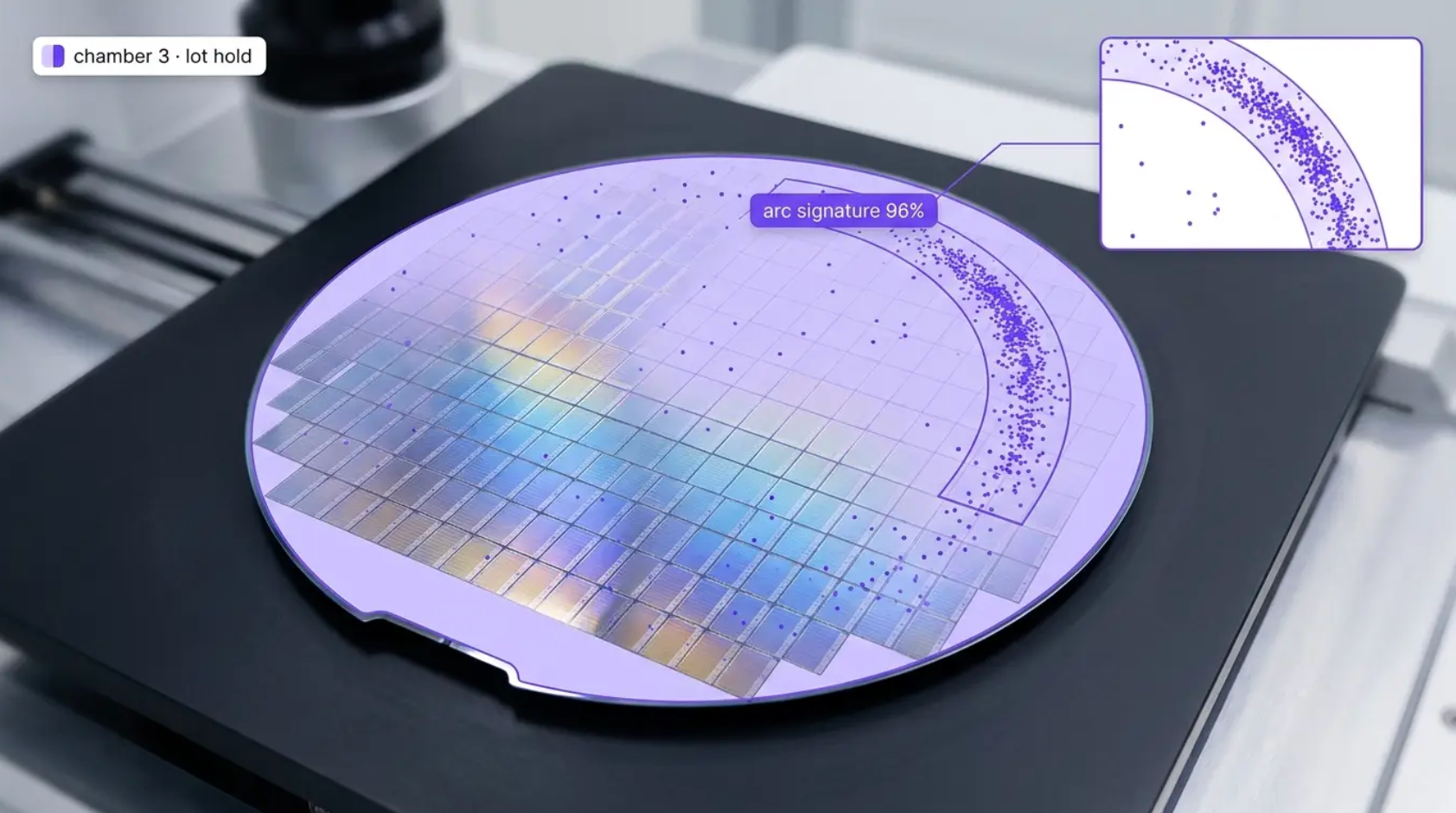
Wafer Defect Detection AI Across Front End, Edge, and Yield

  • Deploy Anywhere, Run Everywhere

    Run wafer defect detection on the edge, on-prem, in your VPC, or via API, wherever your fab's inspection tools, review stations, and yield systems need it.

  • One Platform, Full Adoption

    Tools every fab team can adopt, from tool owners and inspection engineers to defect review analysts, yield engineers, and process integration, no separate ML team required to ship and own classification models.

  • Secure, Compliant, and Audit-Ready

    Data stays safe with SOC 2 Type II compliance, encrypted data, and an uptime SLA, with air-gapped deployment for the fab network and per-wafer records that support ISO 9001, IATF 16949 automotive programs, and customer audits.

  • Defect Detection & Classification
  • Pattern & Litho Defect Flags
  • Edge & Bevel Inspection
  • Backside & Handling Damage
  • Wafer Map Signature Analysis
  • Per-Wafer Yield Records
“Roboflow has been instrumental in accelerating our deployment of innovative AI solutions.”

Travis Turnbull

Vice President & CIO, Pella Corporation

Talk to a vision AI engineer who's shipped wafer defect classification.

A defect review queue that grows faster than the analysts clearing it, a nuisance rate that hides the killer defects inside thousands of false calls, or a spatial signature on the wafer map that named a chamber three lots after it started can mean yield lost to a tool nobody flagged, an excursion caught at probe instead of inline, and review time spent classifying particles that never mattered. Bring us your toughest wafer defect problem and we'll map a working solution.

Ask us about:

  • Solution architecture for fab-network, air-gapped, and automotive-grade environments
  • Live demo on your inspection tool images, review station captures, or wafer maps
  • Deployment options: edge, on-prem, air-gapped, or VPC, with integration into inspection tools, defect databases, and yield management systems
  • ROI modeling against review analyst hours, nuisance rates, excursion detection time, and yield loss per signature

Over 16,000 organizations build with Roboflow.

  • Rivian
  • Pella
  • Chobani
  • USG Corporation
  • BNSF Railway
  • American Woodmark
Start where you are

Vision AI is transforming businesses

Customers across the board are solving complex challenges and driving meaningful impact.

  • Automotive customer

    $10 million

    Saved by automatically detecting defects on the production line

  • Logistics & freight company

    90%

    Less time spent manually tracking shipping inventory

  • Building materials supplier

    60%

    Lower customer return rate with improved product quality

Classify Every Defect and Read the Wafer Map, with Vision AI

Add a classification layer to every inspection with vision AI for wafer defect detection. Built for the fabs where the inspection tool finds ten thousand events a wafer and most of them don't matter, the ones that do are a few pixels of a pattern that isn't quite right, and the spatial signature that names a failing chamber is visible on the wafer map for three lots before anyone connects the dots. Whether you're running front-end inspection, edge and backside checks, or yield analysis, Roboflow classifies every defect and reads every map, with per-wafer records behind every disposition.

Detection and Classification:

  • Classify inspection tool events into real defects and nuisance, cutting the review queue to what matters
  • Catch pattern and litho defects, bridges, opens, missing and extra features, and CD anomalies visible in imagery, at the review station and inline
  • Hold classification across layers, products, and tools, so a new device doesn't reset the model

Edge, Bevel, and Backside:

  • Inspect the edge exclusion zone, bevel, and apex for chips, cracks, and film peeling that seed breakage downstream
  • Detect backside particles, scratches, and chuck marks that become focus spots and hot spots on the next layer
  • Flag handling and transfer damage before it becomes a broken wafer in a tool

Wafer Maps, Yield, and Systems Integration:

  • Read wafer-map spatial signatures, rings, arcs, scratches, center spots, and edge clusters, and match them to the process step and chamber that produce them
  • Trend signatures by tool, chamber, and lot, so an excursion surfaces at inline inspection instead of at probe
  • Integrate with inspection tools, defect databases, and yield management systems, with per-wafer records behind every disposition and every excursion review

Bring intelligence to every wafer today. Stop wafer defects from becoming review backlogs, excursions found at probe, or the chamber signature nobody named until the third lot.

‍

More About Wafer Defect Detection

What is wafer defect detection with Vision AI?

Wafer defect detection with vision AI uses computer vision models to detect and classify defects across the wafer: inspection tool events sorted into real defects and nuisance, pattern and litho defects at the review station, edge, bevel, and backside damage, and wafer-map spatial signatures matched to the process steps and chambers that produce them. Models trained on your actual devices, layers, and tools classify every event, with per-wafer records that support yield programs and automotive-grade documentation.

Can Vision AI cut the defect review queue?

Defect review is the classification hard case: an inspection tool that reports every anomaly it sees, thousands of events per wafer, the killer defects a few pixels of wrong pattern hiding among particles that never mattered, and analysts whose day is spent confirming nuisance. Deep-learning models trained on your actual review images and your own classification history learn what your killers look like on each layer, sort real from nuisance at the review station and inline, hold that judgment across products and tools, and route uncertain events to an analyst instead of guessing, which is how the queue shrinks to what actually threatens yield.

Does this replace our inspection tools and yield management system?

No. Your inspection tools keep finding events, your yield management system keeps the defect database and the correlations, and your metrology keeps CD and overlay. Vision AI adds the layer between them: learned classification that turns events into decisions, pattern judgment on the images your review station already captures, edge and backside coverage where tools are sparse, and wafer-map signature reading that names the chamber while the excursion is still inline. Tool events, model classifications, and yield data land in the same per-wafer record.

Can it integrate with our inspection tools, defect databases, and yield systems?

Yes. Roboflow Inference exposes a standard API and supports common industrial protocols, so classification events flow into your existing systems: inspection and review tools alongside SECS/GEM equipment integration, defect databases and yield management platforms, MES and ERP platforms like SAP and Oracle, and SCADA and HMI platforms like Ignition and AVEVA, through REST, MQTT, OPC UA, and direct database writes. Tool-level integration flags a lot or triggers a review the moment a signature is detected, and every event carries wafer, lot, layer, tool, imagery, and classification, with a full record behind every excursion review.

‍

Stay connected

Get the Latest in Computer Vision First

Unsubscribe at any time. Review our Privacy Policy.