Wafer Surface Defect Detection AI
Catch scratches, particles, and edge chips on every wafer, before the next layer builds on a defect.
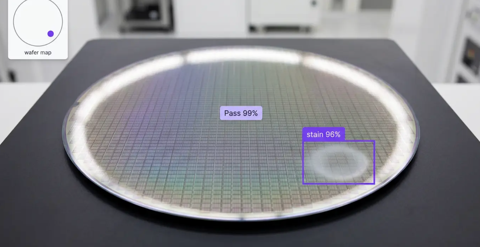
Wafer Surface Defect Detection AI Across Fabs, OSATs, and Wafer Manufacturing
Deploy Anywhere, Run Everywhere
Run wafer surface defect detection on the edge, on-prem, in your VPC, or via API, wherever your fab, probe, and packaging lines need it.
One Platform, Full Adoption
Tools every fab team can adopt, from process and yield engineers to equipment engineers, operators, and quality leads, no separate ML team required to ship and own inspection models.
Secure, Compliant, and Audit-Ready
Data stays safe with SOC 2 Type II compliance, encrypted data, and an uptime SLA, with validation documentation that supports ISO 9001, SEMI-based wafer specifications, and customer qualification and audit requirements.
- Scratch & Micro-Crack Detection
- Particle & Contamination Flags
- Edge Chip & Notch Inspection
- Stain & Discoloration Detection
- Backside & Bare Wafer Inspection
- Lot & Wafer-Level Trend Records
“Roboflow has been instrumental in accelerating our deployment of innovative AI solutions.”
Travis Turnbull
Vice President & CIO, Pella Corporation
Talk to a vision AI engineer who's shipped wafer inspection.
A single scratch that crosses thirty die, cassette of wafers nicked by a worn end effector, or contamination excursion that runs three lots before final test finds it can mean yield loss that multiplies with every layer, a scrapped lot worth a car, or a customer qualification put at risk. Bring us your toughest wafer surface inspection problem and we'll map a working solution.
Ask us about:
- Solution architecture for ISO 9001, SEMI-based specifications, and customer qualification environments
- Live demo on your wafer imagery, macro inspection photos, or edge and backside captures
- Deployment options: edge, on-prem, air-gapped, or VPC, with integration into fab MES, host systems, and yield management
- ROI modeling against scrapped wafers, excursion depth, manual macro inspection time, and escaped handling damage
Over 16,000 organizations build with Roboflow.
- Rivian
- Pella
- Chobani
- USG Corporation
- BNSF Railway
- American Woodmark
Vision AI is transforming businesses
Customers across the board are solving complex challenges and driving meaningful impact.
- Automotive customer
$10 million
Saved by automatically detecting defects on the production line
- Logistics & freight company
90%
Less time spent manually tracking shipping inventory
- Building materials supplier
60%
Lower customer return rate with improved product quality