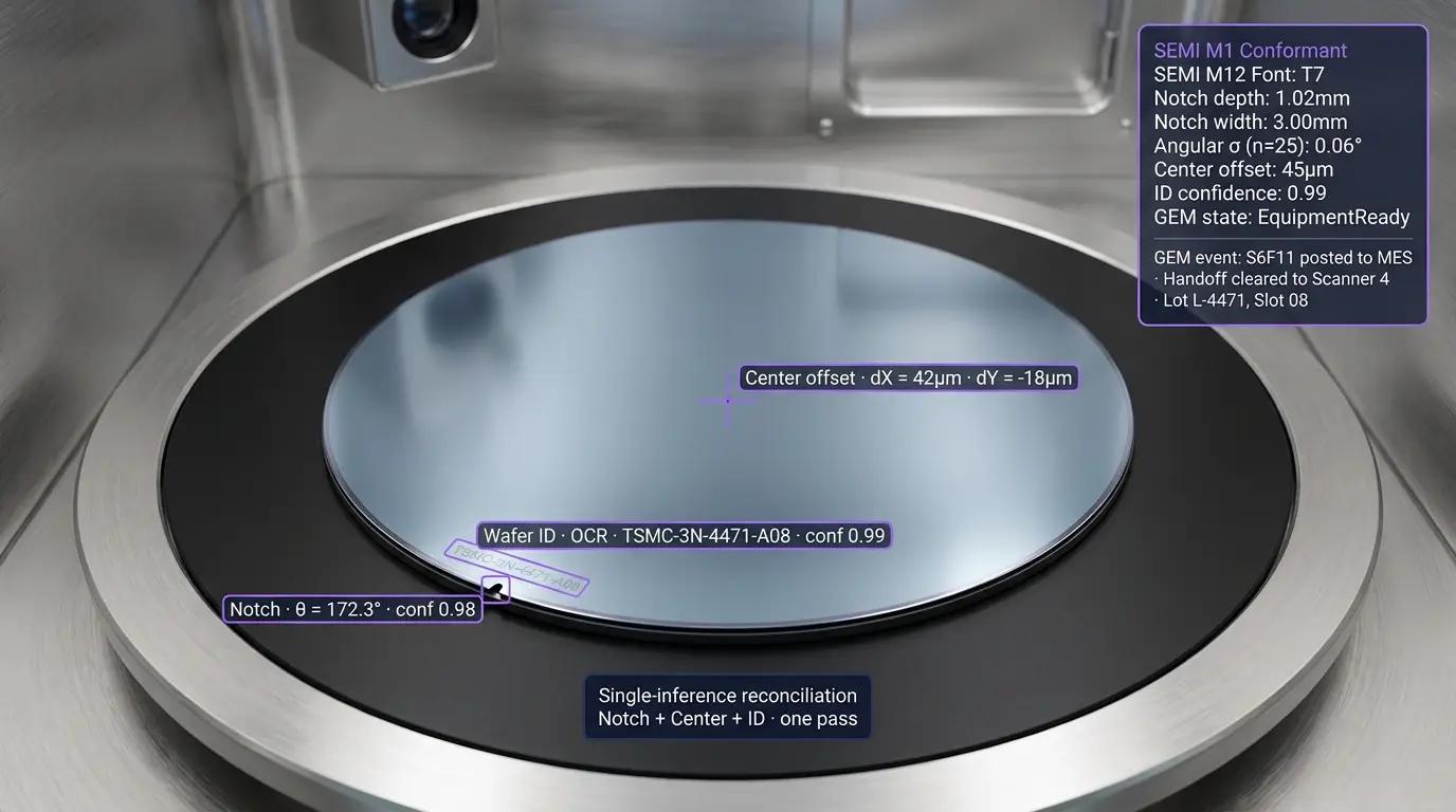
Add a real-time alignment layer to every wafer with Vision AI for wafer notch orientation.
Notch Detection, Angular Orientation, and Wafer-Center Computation:
- Detect the notch on 300mm wafers (SEMI M1: 1mm depth, 3mm width) and the flat on legacy 200mm wafers in a single pass, with sub-degree angular accuracy (typical prealigner requirement below 0.1 degree)
- Compute wafer center offset from prealigner chuck center in the same inference call, so the robot end-effector can pick and load with sub-100 micron accuracy at the tool chuck
- Handle contamination, edge chips near the notch, backside dust, low-contrast notches on polished silicon, film-coated wafers, and patterned wafers where rule-based edge detection returns low confidence or fails outright
Wafer-ID OCR, Batch Verification, and Multi-Tool Deployment:
- Read laser-marked wafer IDs per SEMI M12 (T7 OCR font) and SEMI M13 (T7 hard-mark font) in the same pass as notch detection, tying every physical wafer to its MES/CIM lot record and enabling lot genealogy back to boule and slice
- Verify batch integrity on batch-tool loads: FOUP contents against the expected 25-wafer manifest, wafer sequence, wafer-ID uniqueness, and cross-slot contamination before the process starts
- Deploy on prealigner cameras, EFEM top-down cameras, load-port cameras, wafer inspection stations, and robot end-effector cameras across leading-edge, mature-node, and specialty fabs
SECS/GEM Integration, Cleanroom Safety, and Audit-Ready Records:
- Integrate with SECS-II (SEMI E5), GEM (SEMI E30), HSMS (SEMI E37), and processing management (SEMI E40) so notch-orientation and wafer-ID reads flow into fab MES/CIM (Applied Materials E3, IBM SiView, Siemens Opcenter Camstar, Critical Manufacturing) without custom middleware
- Support ISO 14644 cleanroom deployment (Class 1 through Class 5), SEMI S2 equipment safety, SEMI S8 ergonomics, IEC 62061 functional safety on wafer-handling interlocks, and ITAR/EAR export-control workflows for advanced-node tools with air-gapped inference on tool-side edge hardware
- Log every read with confidence, image crop, notch angle, wafer-center offset, wafer-ID, timestamp, tool ID, and lot ID for SEMI E116 equipment performance tracking, lot-genealogy audit, foundry PPAP submissions, and automotive semiconductor traceability under IATF 16949 and AEC-Q100/Q101
Bring intelligence to every wafer today. Stop notch misses, wafer-ID misreads, and orientation errors from becoming scrapped lots, scanner alignment kills, GEM event halts, or repeat prealigner faults that page out equipment reliability engineers at 3AM.
More About Wafer Notch Orientation
What is wafer notch orientation with Vision AI?
Wafer notch orientation with Vision AI uses computer vision models to detect the notch on 300mm wafers (per SEMI M1) or the flat on legacy 200mm wafers, compute angular orientation to sub-degree accuracy, calculate the wafer center offset from the prealigner chuck center, and read the laser-marked wafer ID (per SEMI M12 and M13) in a single inference call across prealigner, EFEM, FOUP load-port, and inspection cameras.
Can Vision AI hit sub-degree notch orientation with contamination, edge chips, and low-contrast notches?
Yes. Sub-degree notch orientation on wafers with edge chips, backside dust, low-contrast notches on polished silicon, film-coated wafers, and patterned wafers with intense front-side topology is exactly where rule-based edge detection and template-based notch fitting feel the most pressure. Roboflow models are trained on your actual prealigner imagery across your real wafer mix and produce notch-angle and wafer-center estimates with confidence scores that let the EFEM controller decide between attempt, retry, or hand-off to a technician for supervisory review.
Does wafer notch orientation support SEMI M1, M12, M13, E5 (SECS-II), E30 (GEM), and ISO 14644?
Yes. Roboflow models can be trained to support fabs operating under SEMI M1 (silicon wafer specifications, including 300mm notch geometry), SEMI M12 (T7 OCR font for wafer marking), SEMI M13 (T7 hard-mark font), SEMI E5 (SECS-II messaging), SEMI E30 (GEM), SEMI E37 (HSMS), SEMI E40 (processing management), SEMI E116 (Equipment Performance Tracking), SEMI E10 (equipment RAM), SEMI S2 (equipment safety), SEMI S8 (ergonomics), ISO 14644 (cleanroom classification, Class 1 through Class 5), IEC 62061 (functional safety), IATF 16949 (automotive quality), AEC-Q100 (integrated circuit qualification), and AEC-Q101 (discrete semiconductor qualification).
Can it integrate with our EFEM, prealigner, MES/CIM, and SECS/GEM interfaces?
Yes. Roboflow Inference (opens in a new tab) exposes a standard API supporting common semiconductor equipment protocols. Customers integrate with prealigners and EFEMs from Brooks Automation, Rorze, Yaskawa, Sinfonia Technology, Kawasaki, and Kensington, FOUPs from Entegris, Miraial, and Shin-Etsu, wafer-handling robots (Brooks, Yaskawa, Rorze, Kawasaki), fab MES/CIM (Applied Materials E3, IBM SiView, Siemens Opcenter Camstar, Critical Manufacturing), AMHS (Daifuku, Muratec, Shinko), and tool controllers (KLA, Lam Research, ASML, TEL, ASM International, Nikon, Hitachi High-Tech) through native SECS/GEM protocols plus REST, MQTT, OPC UA, and direct database writes, with tool-controller-level pass/fail on borderline confidence, GEM event generation on retry conditions, and SEMI E116 EPT records.