Semiconductor OCR AI

Read every laser-marked wafer ID, reticle ID, FOUP ID, and chip package datecode.
Shipping container with OCR output

Semiconductor OCR AI Across Wafer ID, Reticle, FOUP, Chip Package, and Every Semi-Fab Traceability Task

Deploy Anywhere, Run Everywhere

Run semiconductor OCR on the edge (line-side jetson-class or industrial edge in the fab), on-prem in the fab data center, in a customer-controlled VPC, or air-gapped for advanced-node process tools.

One Platform, Full Adoption

Tools every semiconductor manufacturing team can adopt, no separate machine learning team required.

Built for SEMI Standards, Automotive AEC-Q, MIL-STD, and Every Semi Traceability Standard

SOC 2 Type II, encrypted data, and an uptime SLA on every tool.
Front-Side Wafer ID (SEMI M12 T7 Font)
Backside Hard-Mark (SEMI M13)
Reticle & FOUP Carrier ID Reading
Chip Package OCR at OSAT (BGA, QFN, LGA, μBGA)
SECS/GEM MES Integration (E5, E30, E37)
Automotive AEC-Q100 & MIL-STD-883 Traceability
Front-Side Wafer ID (SEMI M12 T7 Font)
Backside Hard-Mark (SEMI M13)
Reticle & FOUP Carrier ID Reading
Chip Package OCR at OSAT (BGA, QFN, LGA, μBGA)
SECS/GEM MES Integration (E5, E30, E37)
Automotive AEC-Q100 & MIL-STD-883 Traceability
Front-Side Wafer ID (SEMI M12 T7 Font)
Backside Hard-Mark (SEMI M13)
Reticle & FOUP Carrier ID Reading
Chip Package OCR at OSAT (BGA, QFN, LGA, μBGA)
SECS/GEM MES Integration (E5, E30, E37)
Automotive AEC-Q100 & MIL-STD-883 Traceability
Front-Side Wafer ID (SEMI M12 T7 Font)
Backside Hard-Mark (SEMI M13)
Reticle & FOUP Carrier ID Reading
Chip Package OCR at OSAT (BGA, QFN, LGA, μBGA)
SECS/GEM MES Integration (E5, E30, E37)
Automotive AEC-Q100 & MIL-STD-883 Traceability

Talk to a Vision AI engineer who's shipped semiconductor OCR.

A single misread wafer ID at a 300mm prealigner, a wrong-orientation load into a lithography scanner, or a chip package datecode misread at OSAT burn-in can mean a scrapped lot that costs $50,000+ per wafer at leading edge, a scanner alignment error that kills a full run, or an AEC-Q100 automotive traceability gap that a tier-one supplier catches on the next PPAP audit. Bring us your toughest semiconductor OCR problem and we'll map a working solution.
  • Solution architecture for SEMI M12, M13, M1, E5 (SECS-II), E30 (GEM), E37 (HSMS), E40, E116, E10, S2, S8, ISO 14644, IEC 62061, IATF 16949, AEC-Q100/Q101/Q200, AS9100, MIL-STD-883, MIL-PRF-31032/38534/38535/19500, IPC-1782, ITAR/EAR export controls, and customer-specific tool qualification acceptance criteria
  • Live demo on your real prealigner footage, EFEM top-down video, reticle stocker imagery, FOUP load-port capture, wafer-sorter imagery, chip package OCR from OSAT test and burn-in stations, in your real cleanroom lighting and wafer-mix conditions (bare silicon, patterned, film-coated, backside-marked returns, low-contrast laser marks)
  • Deployment options: prealigner, EFEM, FOUP load-port, reticle stocker, wafer sorter, chip package OCR station, burn-in board, test board, robot end-effector, edge (fab-side jetson-class or industrial edge), on-prem, air-gapped for advanced-node process tools, with integration into SECS/GEM interfaces, EFEM controllers, fab MES/CIM (Applied Materials E3, IBM SiView, Siemens Opcenter Camstar, Critical Manufacturing), and OSAT test-cell controllers
  • ROI modeling against scrapped lots at leading-edge cost ($50k+ per wafer), scanner alignment kills, repeat wafer-ID misreads driving equipment reliability engineer overtime, GEM event downtime, AEC-Q100 traceability audit exposure, chip package datecode misreads at OSAT burn-in cascading into tier-one supplier PPAP rejections, and hardware refresh on aging dedicated OCR systems
We will connect you with an AI subject matter expert on our team based on your answers.
What challenges would you like to solve with vision AI?
Where will you run vision AI?
Are you replacing a current solution with AI or will this be a new solution?
How many detections do you anticipate per month?
Describe the business problem you would like to solve.
Oops! Something went wrong while submitting the form.

Over 16,000 organizations build with Roboflow.

“Roboflow has been instrumental in accelerating our learning and deployment of innovative AI solutions”
Travis Turnbull Vice President & CIO, Pella Corporation
See customer stories
Trusted by top manufacturers

Read Every Wafer, Every Reticle, and Every Chip Package, from Prealigner to OSAT Burn-In, with Vision AI

Add a real-time OCR layer to every wafer, reticle, and chip package across your fab and OSAT lines with Vision AI for semiconductor OCR. Roboflow reads front-side and backside wafer IDs, reticle IDs, FOUP carrier IDs, and chip package marks at prealigners, EFEMs, load ports, and OSAT test cells, and connects those reads to your MES, AMHS, and tool controllers.

Front-Side and Backside Wafer ID Reading (SEMI M12 and M13):

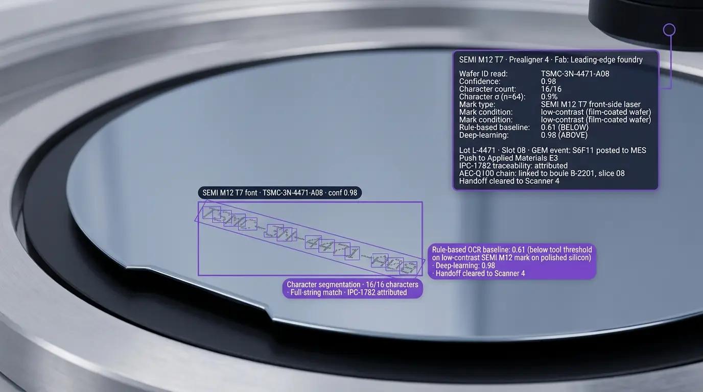
  • Read front-side laser-marked wafer IDs at prealigners on 200mm and 300mm wafers with sub-pixel accuracy on low-contrast marks, patterned wafers, film-coated wafers, and edge-chip returns, plus backside hard-marked IDs on rougher surfaces where mark depth and edge quality vary
  • Handle the hard cases: low-contrast laser marks, backside dust and contamination, edge chips near the mark, laser-mark drift, and returned wafers with cleaning-cycle wear
  • Compute wafer center, notch angle, and wafer ID in a single inference call at the prealigner, tying every wafer to its MES record for full lot genealogy back to boule, slice, and vendor lot

Reticle IDs, FOUP Carrier IDs, and OSAT Chip Package OCR:

  • Read reticle IDs on glass substrates at reticle stockers, preventing wrong-reticle loads at ASML, Nikon, or Canon scanners that would burn a run
  • Read FOUP carrier IDs at 300mm load ports and 200mm SMIF pod IDs, preventing wrong-carrier loads and feeding SECS/GEM events to the AMHS
  • Read chip package datecodes and lot IDs at OSAT test and burn-in on BGA, QFN, LGA, WLCSP, and μBGA packages (down to 0.15mm characters) at up to 60,000 units per hour

SECS/GEM Integration, Cleanroom Deployment, and Compliance:

  • Integrate with SECS-II (E5), GEM (E30), HSMS (E37), and processing management (E40) so reads flow into fab MES/CIM (Applied Materials E3, IBM SiView, Siemens Opcenter Camstar, Critical Manufacturing) and OSAT test-cell controllers without custom middleware
  • Support ISO 14644 cleanrooms (Class 1-5), SEMI S2 and S8 safety and ergonomics, IEC 62061 functional safety, IPC-1782 traceability, and ITAR/EAR air-gapped deployment for advanced-node tools
  • Log every OCR read with confidence, image, character segmentation, timestamp, tool, lot, wafer or FOUP or reticle ID, and operator for SEMI E116 tracking, IPC-1782 genealogy, automotive AEC-Q100/Q101/Q200, and aerospace MIL-STD-883 and MIL-PRF-38534/38535/19500 qualification

Bring intelligence to every wafer, reticle, and chip today.

More About Semiconductor OCR

What is semiconductor OCR with Vision AI?

Semiconductor OCR with Vision AI uses computer vision models to read every ID on every wafer, reticle, carrier, and chip package. That includes front-side laser marks (SEMI M12) and backside hard marks (SEMI M13) on 200mm and 300mm wafers, reticle IDs on glass, FOUP and SMIF pod IDs at load ports, and package marks on BGA, QFN, LGA, WLCSP, and μBGA down to 0.15mm characters at up to 60,000 units per hour. Reads flow into fab MES (Applied Materials E3, IBM SiView, Siemens Opcenter Camstar, Critical Manufacturing) through native SECS/GEM. Leading-edge and memory fabs, foundries, IDMs, specialty fabs, and OSAT providers use it to prevent scrapped lots ($50K+ per wafer at leading edge), avoid scanner alignment kills, cut wafer-ID misreads, and keep automotive and aerospace traceability intact.

Can Vision AI read low-contrast wafer marks, film-coated wafers, and 0.15mm μBGA characters at OSAT speed?

Yes. Rule-based OCR readers work well on high-contrast printed labels at a known angle but drop confidence on low-contrast laser marks on polished silicon, film-coated wafers, sub-millimeter characters, laser-mark drift over the tool's mark lifecycle, and backside dust or edge chips that create false character candidates. Roboflow models are trained on your actual prealigner, reticle-stocker, load-port, and OSAT imagery across your real wafer and package mix, producing character-by-character reads with confidence scores that let the EFEM, reticle stocker, load port, or test handler decide between accept, retry, or hand-off to a technician.

Does semiconductor OCR support SEMI M12, M13, SECS-II, GEM, and MIL-STD-883?

Yes. Roboflow supports fabs and OSAT lines operating under SEMI M12, M13, M1, E5 (SECS-II), E30 (GEM), E37 (HSMS), E40, E116, E10, E23, S2, S8, and E15.1, ISO 14644 cleanroom classes, IEC 62061 functional safety, IPC-1782 traceability, IATF 16949 and AEC-Q100/Q101/Q200 automotive, AS9100 aerospace, and MIL-STD-883 and MIL-PRF-31032/38534/38535/19500 defense qualification. Every read is logged with confidence, image, character segmentation, timestamp, tool, and lot, ready for tool qualification, foundry PPAP, automotive audits, aerospace and defense qualification, and IPC-1782 lot genealogy.

Can it integrate with our SECS/GEM, EFEM, MES/CIM, and OSAT test handlers?

Yes. Roboflow Inference exposes a standard API. Customers integrate with prealigners and EFEMs (Brooks Automation, Rorze, Yaskawa, Sinfonia, Kensington, Kawasaki), FOUPs (Entegris, Miraial, Shin-Etsu), reticle stockers (Hirata, Rorze, Muratec), OSAT test handlers (Advantest, Cohu, Aetrium, Boston Semi Equipment, Multitest), burn-in systems (Aehr, DES Group, Micro Control), fab MES/CIM, AMHS (Daifuku, Muratec, Shinko), and tool controllers (KLA, Lam Research, ASML, TEL, ASM International, Nikon, Hitachi High-Tech, Onto Innovation) through native SECS/GEM plus REST, MQTT, OPC UA, and direct database writes. Deployments run on-prem, at the tool edge, in a VPC, or air-gapped, with pass/fail decisions to the tool controller, GEM event generation, SEMI E116 EPT records, and IPC-1782 genealogy for foundry PPAP and mil-spec supplier records.

Stay Connected

Get the Latest in Computer Vision First

Thank you for subscribing!
Oops! Something went wrong!.
Unsubscribe at any time. Review our Privacy Policy.

Additional resources

Vision AI is transforming every industry. Let’s transform yours.