PCB Defect Detection AI

Catch tombstoning, solder bridges, missing components, polarity errors, lifted leads, and trace defects across every PCBA on the line, before defects ship to your OEM.
Shipping container with OCR output

PCB Defect Detection AI Across SMT, Through-Hole, Soldering, and Final QC

Deploy Anywhere, Run Everywhere

Run PCB defect detection on SMT line AOI co-pilot stations, post-reflow inspection cells, post-wave solder inspection, through-hole assembly cells, final QC checkpoints, and rework station verification, on the edge, on-prem, in your VPC, or via API, wherever your electronics manufacturing line needs it.

One Platform, Full Adoption

Tools every electronics manufacturing team can adopt, from SMT process engineers, AOI and AVI operators, and PCBA quality engineers to plant managers, manufacturing engineering, and operations leadership at electronics manufacturers, EMS providers, and OEM in-house electronics operations, no separate ML team required to ship and own defect detection models for every PCBA program.

Built for Electronics Manufacturing Standards and Audit-Ready Records

Update inspection logic in minutes when boards, BOMs, or rework criteria change, with audit-ready records that support IPC-A-610 (Acceptability of Electronic Assemblies), IPC-A-600 (Acceptability of Printed Boards), J-STD-001 (Soldering Requirements), IPC-7711 and IPC-7721 (Rework and Repair), IATF 16949 for automotive electronics, AS9100 for aerospace electronics, ISO 13485 for medical electronics, and customer-specific PPAP and APQP documentation. SOC 2 Type II compliance, encrypted data, HIPAA compliance, and an uptime SLA on every deployment.
Tombstoning & Billboarding Detection
Solder Bridge & Short Detection
Missing & Wrong Component Detection
Polarity, Orientation & Lifted Lead
Insufficient Solder & Solder Void
Trace Defect & PCB Scratch
Tombstoning & Billboarding Detection
Solder Bridge & Short Detection
Missing & Wrong Component Detection
Polarity, Orientation & Lifted Lead
Insufficient Solder & Solder Void
Trace Defect & PCB Scratch
Tombstoning & Billboarding Detection
Solder Bridge & Short Detection
Missing & Wrong Component Detection
Polarity, Orientation & Lifted Lead
Insufficient Solder & Solder Void
Trace Defect & PCB Scratch
Tombstoning & Billboarding Detection
Solder Bridge & Short Detection
Missing & Wrong Component Detection
Polarity, Orientation & Lifted Lead
Insufficient Solder & Solder Void
Trace Defect & PCB Scratch

Talk to a Vision AI engineer who's shipped PCB defect detection on the SMT line.

A single missed tombstoned chip, undetected solder bridge, or polarity error on a polarized capacitor can mean a field-return event, an automotive electronics recall on a deployed program, or a customer chargeback that hits your margin and reputation. Bring us your toughest PCB defect detection problem and we'll map a working solution.
  • Solution architecture for IPC-A-610, IPC-A-600, J-STD-001, IPC-7711 and IPC-7721, IATF 16949, AS9100, ISO 13485, and customer-specific PPAP and APQP environments
  • Live demo on your AOI imagery, post-reflow inspection footage, post-wave solder video, or finished PCBA samples
  • Deployment options: edge, on-prem, air-gapped, robot-mounted, or VPC, with integration into AOI and AVI systems, SMT line PLCs, MES, and ERP
  • ROI modeling against rework, scrap, field returns, customer chargebacks, and recall risk on board-level defects
  • We will connect you with an AI subject matter expert on our team based on your answers.
    What challenges would you like to solve with vision AI?
    Where will you run vision AI?
    Are you replacing a current solution with AI or will this be a new solution?
    How many detections do you anticipate per month?
    Describe the business problem you would like to solve.
    Oops! Something went wrong while submitting the form.

    Over 16,000 organizations build with Roboflow.

    “Roboflow has been instrumental in accelerating our learning and deployment of innovative AI solutions”
    Travis Turnbull Vice President & CIO, Pella Corporation
    See customer stories
    Trusted by top manufacturers

    Catch Every PCBA Defect from First Component Place Through Final Inspection, with Vision AI

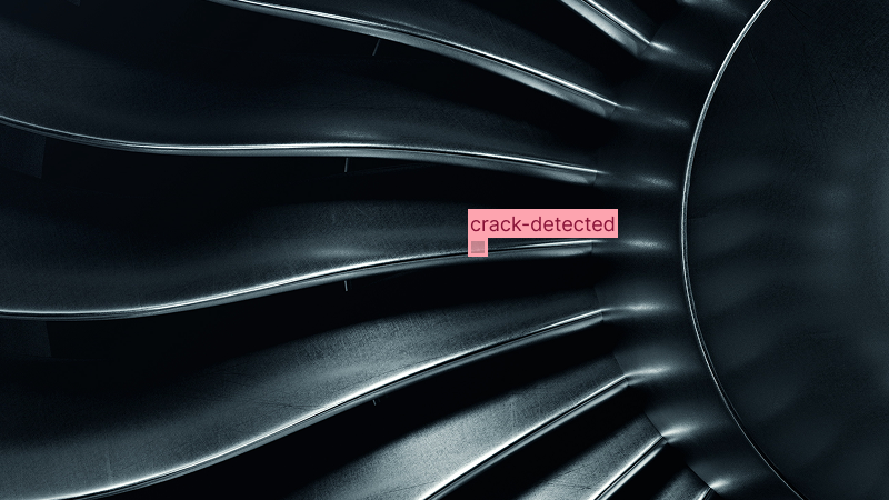
    Add a real-time inspection layer to every PCBA on the line with Vision AI for PCB defect detection. Built for the operations where one missed tombstoned chip resistor, solder bridge between adjacent pads, missing component on a high-density board, polarity error on a polarized capacitor, lifted lead on a SOIC or QFP, insufficient solder joint, or PCB trace defect can mean a field-return event, an automotive electronics recall on a deployed program, a customer chargeback that hits your margin and reputation, or a regulatory enforcement action on a regulated electronics program (medical, aerospace, automotive). Whether you're inspecting post-paste solder paste deposition, post-place pre-reflow component placement, post-reflow AOI on populated boards, post-wave solder for through-hole, BGA underside coordinated with X-ray, or finished PCBA before final pack-out, Roboflow extends your QC coverage to every board on the line, on the AOI and AVI inspection stations your facility already runs.

    SMT and Surface Mount Defect Detection:

    • Catch tombstoning, billboarding, lifted leads, and skewed component placement on chip passives (0402, 0603, 0805), QFN, SOIC, QFP, and BGA packages
    • Detect solder bridges between adjacent pads, insufficient solder volume, solder voids, and cold joints across every populated board
    • Verify component presence, correct part value, polarity orientation on polarized capacitors and ICs, and correct reference designator match across the BOM

    Through-Hole, Wave Solder, and Trace Defects:

    • Verify through-hole component placement, lead clinching, and wave solder joint integrity on every connector, transformer, and through-hole part
    • Catch PCB trace defects (open traces, short traces, copper scratches, solder mask defects) on the bare board and on populated boards
    • Detect via and pad defects, gold finger contamination, and silkscreen reference designator errors that affect rework traceability

    AOI Co-Pilot, Standards Compliance, and Field-Return Defense:

    • Co-pilot existing AOI and AVI systems (Koh Young, ViTrox, Saki, Mirtec, Test Research Inc, Omron) with deep-learning visual verification on borderline rejects to reduce false-positive scrap and increase true-positive confidence on safety-critical assemblies
    • Maintain validated inspection records that support IPC-A-610 (Acceptability of Electronic Assemblies), IPC-A-600 (Acceptability of Printed Boards), J-STD-001 (Soldering Requirements for Electrical and Electronic Assemblies), IPC-7711 and IPC-7721 (Rework and Repair), IATF 16949 for automotive electronics, AS9100 for aerospace electronics, and ISO 13485 for medical electronics
    • Trigger line-level reject and rework-station routing in real time through PLC and MES integration when inspection criteria fail, with full audit trail for customer audits, automotive electronics PPAP submissions, and field-return investigation

    Bring intelligence to every PCBA today. Stop board-level defects from becoming field returns, automotive electronics recalls, or customer chargebacks.

    More About PCB Defect Detection

    What is PCB defect detection with Vision AI?

    PCB defect detection with Vision AI uses computer vision models to inspect printed circuit board assemblies at every stage of electronics manufacturing, from post-paste solder paste deposition through post-place pre-reflow component placement, post-reflow automated optical inspection (AOI) on populated boards, post-wave solder for through-hole assemblies, BGA underside inspection coordinated with X-ray, and finished PCBA before final pack-out. The system extends QC coverage to every board on the line, catching tombstoning and billboarding on chip passives, solder bridges between adjacent pads, missing components and wrong-value components, polarity errors on polarized capacitors and ICs, lifted leads on SOIC and QFP packages, insufficient solder volume and solder voids, cold joints, PCB trace defects (open traces, short traces, copper scratches, solder mask defects), and silkscreen reference designator errors that affect rework traceability. Electronics manufacturers, EMS providers (Foxconn, Flex, Jabil, Sanmina, Celestica), and OEM in-house electronics operations use it to cut rework, prevent field returns, reduce customer chargebacks, defend against automotive electronics recalls, and document compliance under IPC-A-610, IPC-A-600, J-STD-001, IPC-7711 and IPC-7721, IATF 16949 for automotive electronics, AS9100 for aerospace electronics, and ISO 13485 for medical electronics.

    Can Vision AI catch the defects existing AOI systems miss?

    Yes. Tombstoning, billboarding, lifted leads, and subtle solder joint defects on high-density mixed-technology boards are exactly where existing rule-based and template-matching AOI systems feel the most pressure. Rule-based AOI excels at deterministic measurement tasks with high-contrast features, fixed lighting, and consistent component presentation (precise dimensional measurement of solder fillet height with 3D AOI, barcode and reference designator OCR on uniform silkscreen), but struggles with morphological variation (subtle component skew that varies lot to lot, solder joint variation from reflow profile drift), color and reflectivity variation from solder finish lot to lot, SKU complexity across hundreds of board variants and BOM revisions, and high-density placement where templating fails. Roboflow models add a deep-learning inspection layer trained on your actual board appearance, lot variation, and BOM revision differences, catching the defect categories rule-based AOI struggles with and co-piloting existing AOI and AVI installations from Koh Young, ViTrox, Saki, Mirtec, and Omron by adding visual verification on borderline rejects (reducing false-positive scrap from over-sensitive thresholds, increasing true-positive confidence on safety-critical assemblies destined for automotive, aerospace, or medical programs).

    Does PCB defect detection support IPC-A-610, J-STD-001, and IATF 16949?

    Yes. Roboflow models can be trained against your specific IPC-A-610 (Acceptability of Electronic Assemblies, the universal electronics assembly acceptance standard covering Class 1, Class 2, and Class 3 quality levels), IPC-A-600 (Acceptability of Printed Boards, covering bare PCB acceptance criteria), J-STD-001 (Requirements for Soldered Electrical and Electronic Assemblies, the universal soldering standard), IPC-7711 and IPC-7721 (Rework, Modification and Repair of Electronic Assemblies), IATF 16949 for automotive electronics quality management, AS9100 and AS9110 for aerospace electronics quality management, ISO 13485 for medical electronics quality management, ESD S20.20 for electrostatic discharge control, and customer-specific PPAP (Production Part Approval Process) and APQP (Advanced Product Quality Planning) acceptance criteria for automotive electronics programs. The system applies the same pass/fail logic your trained IPC-certified inspectors use, against your written specifications, AOI acceptance criteria, and customer board release documentation, and produces validated inspection records that support customer audits, automotive Tier 1 PPAP submissions, field-return investigations, regulatory enforcement defense on medical and aerospace electronics, and IPC Class 3 traceability for safety-critical programs. Your IPC compliance and quality teams own the acceptance criteria; Roboflow provides the inspection engine that enforces them at line speed across every board.

    Can it integrate with our AOI systems, SMT line PLCs, MES, eQMS, and ERP?

    Yes. Roboflow Inference exposes a standard API and supports common electronics manufacturing automation protocols, so Vision AI PCB defect detection events flow into your existing AOI and AVI systems, SMT line PLCs, MES, eQMS, ERP, and field-return traceability platforms. Customers integrate with AOI and AVI systems from Koh Young, ViTrox, Saki, Mirtec, Test Research Inc, and Omron, SMT placement equipment from ASMPT (SIPLACE), Fuji, Yamaha, Panasonic, and Hanwha, reflow ovens from Heller, Vitronics Soltec, and BTU, X-ray systems from Yxlon, Nordson DAGE, and Nikon, SMT MES platforms (Cogiscan, Aegis FactoryLogix, Critical Manufacturing, iTAC), eQMS platforms (MasterControl, Veeva Vault QMS, Sparta TrackWise, ETQ Reliance), and ERP systems (SAP, Oracle) through REST, MQTT, OPC UA, and direct database writes, with PLC-level integration to SMT line conveyors, AOI gate decisions, and rework station routing where pass/fail decisions need to drive line behavior or downstream sorting. Models support full IQ/OQ/PQ documentation, audit trails for training data, model versions, and inspection results that pass customer audits, automotive Tier 1 PPAP submissions, IPC Class 3 audits, field-return investigation requirements, and medical and aerospace electronics regulatory enforcement defense.

    Stay Connected

    Get the Latest in Computer Vision First

    Thank you for subscribing!
    Oops! Something went wrong!.
    Unsubscribe at any time. Review our Privacy Policy.

    Additional resources

    Vision AI is transforming every industry. Let’s transform yours.